CVD Waveform Steps
CVD :: Capacitive Voltage Divider
DAC :: Digital-to-Analog Converter
ADC :: Analog-to-Digital Converter
TAD :: Time required for the ADC to complete one bit conversion.
-
Stage 1 (a) :: Pre-charge
- The sensor is set to output low.
-
Either:
- The DAC is set to VDD and the ADC mux is pointed to the DAC.
- Another analog channel is set as output high and the ADC mux is pointed to that channel.
- (Delay, based on CVD_CHOLD_CHARGE_DELAY)
-
Stage 2 (a) :: Acquisition / Settling
- The sensor is set to an input.
- The ADC mux is updated to point to the sensor.
- (Delay, based on CVD_SETTLING_DELAY)
-
Stage 3 (a) :: Sampling
- The ADC's GO/nDONE bit is set.
- The ADC mux waits 1/2 TAD then disconnects from the sensor.
- (The mTouch framework automatically delays the necessary time for the mux to disconnect.)
- The sensor is set to an output.
The ADC conversion completes while math is being performed on the previous mTouch scan result.
-
Stage 1 (b) :: Pre-charge
- The sensor is set to output high.
-
Either:
- The DAC (digital-to-analog converter) is set to VSS and the ADC (analog-to-digital converter) mux is pointed to the DAC.
- Another analog channel is set as output low and the ADC mux is pointed to that channel.
- (Delay, based on CVD_CHOLD_CHARGE_DELAY)
-
Stage 2 (b) :: Acquisition / Settling
- The sensor is set to an input.
- The ADC mux is updated to point to the sensor.
- (Delay, based on CVD_SETTLING_DELAY)
-
Stage 3 (b) :: Sampling
- The ADC's GO/nDONE bit is set.
- The ADC mux waits 1/2 TAD then disconnects from the sensor.
- (The mTouch framework automatically delays the necessary time for the mux to disconnect.)
- The sensor is set to an output.
The ADC conversion completes. When finished, the first scan is subtracted from the second. The second scan is offset by 1024 to make sure this subtract never goes negative.
CVD Waveform Steps
Below is a picture of what the CVD waveform should look like on a scope. Note that sensor lines are used both for scanning themselves and the other sensors. You may notice the sensor being pulled high and low during other sensor's scans.
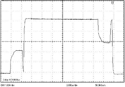
The mTouch framework provides the ability to tune the timing of CVD waveform for specific hardware designs. The amount of parasitic capacitance, the size of the sensor, the size of the sensor's series resistor, and VDD all play a role in determining the amount of time required to charge/discharge during each step of the scan.
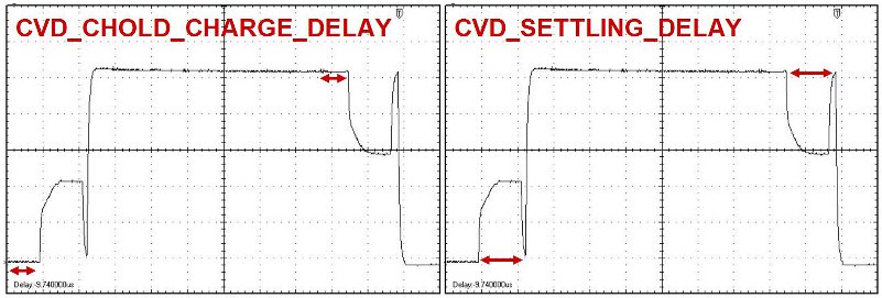
CVD Waveform Delay Configuration Options
- CVD_CHOLD_CHARGE_DELAY
This value determines the amount of time provided for charging the internal hold capacitor of the ADC.
If this value is too small: There will be noticable crosstalk between closely-indexed sensors that is not related to the hardware layout of the application.
If this value is too large: The mTouch ISR will take an unnecessarily long amount of time to execute.
To correctly set this value:- Set this value to 0, compile and program.
-
Look at the raw values on the mTouch One-Way GUI or through a terminal program.
You can find the mTouch One-Way GUI inYour MLA Directory/mTouchCapDemos/Utilities/PIC12F PIC16F Utilities/mTouch One-Way GUI -
Produce the largest shift possible on the sensor with the highest amount of capacitance by pressing on it. ("Highest Capacitance" usually corresponds to the sensor with the highest unpressed raw value.)
- Do you notice a strange crosstalk behavior on a different sensor? If no, leave this value to 0. If yes...
- Increase the delay until the crosstalk behavior is eliminated.
Once you've solved the crosstalk for the sensor with the highest amount of capacitance, the others will be fine as well and you have correctly tuned the Chold delay time.
- CVD_SETTLING_DELAY
This value determines the amount of time provided for the external sensor and internal hold capacitor to charge-average their voltages.
If this value is too small: The sensors will not be as sensitive as they could be and your sensor's readings will be VDD dependant.
If this value is too large: The noise immunity of the system will not be as robust as it could be.
To correctly set this value:- Set this value to 0, compile and program.
-
Look at the raw values on the mTouch One-Way GUI or through a terminal program while powering the system at the desired VDD level.
You can find the mTouch One-Way GUI inYour MLA Directory/mTouchCapDemos/Utilities/PIC12F PIC16F Utilities/mTouch One-Way GUI -
Adjust VDD by plus and minus 0.5V
- Do you notice any change in the unpressed value as VDD is changing? If no, leave this value alone. If yes...
- Increase the delay until the sensor's reading no longer changes as VDD changes.
Once this has occurred, the settling time has been correctly tuned to provide the maximum amount of sensitivity while minimizing the framework's susceptibility to noise.