The framework is designed to output a synchronous signal on another pin to help maximize the sensitivity of the mTouch sensors. A guard ring is most effective when it encloses a sensor and shields it from any nearby communication traces, power planes (including ground), antennas, or other noise sources. The theory is that we want to decrease the voltage differential between the capacitive sensor and its environment.
- Note:
- One guard ring can be shared among all sensors.
How It Works
Guard rings (or shields) are driven by an I/O or the DACOUT pin to minimize the amount of parasitic capacitance on the sensor. Parasitic capacitance will cause the field lines of the sensor to be distorted - pulling them down and decreasing the amount of sensitivity. With the guard ring, however, the sensor will be shielded from this effect.
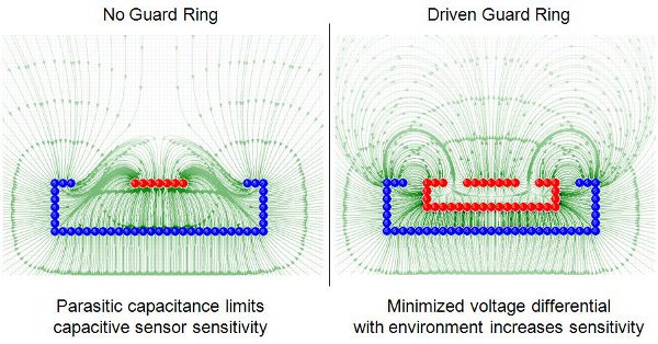
Sensor Field Lines with and without a Guard Ring
Guard Ring / Shield Configuration
There are two possible ways to implement the guard ring.
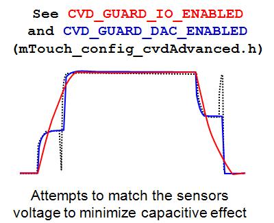
Two Guard Options and Their Behaviors
To implement the blue line (maximum sensitivity gain), the DACOUT pin must be connected to the guard ring on your board. This is the easiest and most fine-tunable of the two options.
- Open the mTouch_config_cvdAdvanced.h file and uncomment CVD_GUARD_DACOUT_ENABLED
- Define CVD_GUARD_DACCON0_A with the value of DACCON0 during the settling phase of the first sample.
- Define CVD_GUARD_DACCON1_A with the value of DACCON1 during the settling phase of the first sample.
- Define CVD_GUARD_DACCON0_B with the value of DACCON0 during the settling phase of the second sample.
-
Define CVD_GUARD_DACCON1_B with the value of DACCON1 during the settling phase of the second sample. 'A' refers to the first half of the CVD scan when the external sensor is held low, the internal hold capacitor is charged high, and then they are connected. 'B' refers to the second half where the reverse is true. The settling voltage may be different for each of these, so different DACCON values may be required.
 #define CVD_GUARD_DACOUT_ENABLED
 #define CVD_GUARD_DACCON0_A     PIC_DACOUT_DACCON0_HALF_VDD    // Pre-defined value to set '1/2 VDD'
 #define CVD_GUARD_DACCON1_A     PIC_DACOUT_DACCON1_HALF_VDD    // Pre-defined value to set '1/2 VDD'
 #define CVD_GUARD_DACCON0_B     PIC_DACOUT_DACCON0_HALF_VDD    // Pre-defined value to set '1/2 VDD'
 #define CVD_GUARD_DACCON1_B     PIC_DACOUT_DACCON1_HALF_VDD    // Pre-defined value to set '1/2 VDD'
To implement the red line, any I/O pin may be used. A large amount of series resistance should be added to the pin to lower the rise/fall time of the pin. The closer the rise/fall time of the I/O is able to match the rise/fall of the mTouch sensor, the better the result. Good typical starting value: 100K-200K ohms.
- Open the mTouch_config_cvdAdvanced.h file and uncomment CVD_GUARD_IO_ENABLED
- Define CVD_GUARD_PORT with the LAT or PORT register for your output pin.
-
Define CVD_GUARD_PIN with the LAT or PORT bit that will access the output pin.
 #define CVD_GUARD_IO_ENABLED
 #define CVD_GUARD_PORT        LATA        // <-- Guard ring is connected to RA2 / LATA2
 #define CVD_GUARD_PIN         2