Getting Started: Smart Card Demo
Configuration
3: Low Pin Count USB Development Kit
Configuration
4: PICDEM FS USB
Configuration
3: PIC18F14K50 + LPC Board
Configuration
4: PICDEM FS USB
Required Hardware:
To run this project, you will need one of the
following sets of hardware:
Configuration 1: HPC Explorer
High
pin count (HPC) Explorer (DM183022)
SC (Smart/Sim Card) PICTail Board
And
one of the following PIMs
PIC18F87J50
Plug-In-Module (PIM) (MA180021)
PIC18F46J50
Full Speed USB Demo Board (MA180024)
Configuration 2: Explorer 16
Explorer
16 (DM240001)
SC
(Smart/Sim Card) PICTail Board
And one of the following PIMs
PIC24FJ256GB110 Plug-In-Module (PIM) (MA240014),
PIC32MX795F512L Plug-In-Module (PIM) (MA320003),
dsPIC33FJ128MC710,
PIC24HJ256GP610
Configuration 3: Low Pin Count USB Development Kit
Low Pin Count USB Development Kit with PICKit 2
Debugger/Programmer (DV164126)
or without
Debugger/Programmer (DM164127).
SC (Smart/Sim Card) PICTail Board
Configuration 4: PICDEM FS USB
PICDEM
FS USB (DM163025)
SC (Smart/Sim Card) PICTail Board
Configuring the Hardware:
This
section describes how to set up the various configurations of hardware to run
this demo.
Configuration 3: PIC18F14K50 + LPC Board
Configuration 4: PICDEM FS USB Board
Configuration 1: HPC Explorer
1)
Before inserting PIC18F87J50 PIM or PIC18F46J50 PIM in the HPC Explorer board,
insure that the processor selector switch (S3) is in the “ICE” position as seen
in the image below. Failure to so will
result in difficulties in getting the PIC18F87J50/PIC18F46J50 PIM to sit
properly on the HPC Explorer.
2)
Before inserting PIC18F87J50/PIC18F46J50 PIM into the HPC Explorer board,
remove all the attached cables from both the boards. Be careful while inserting
the PIM into HPC board. Insure that no pins are bent or damaged during the process. Also insure that the PIM is not shifted in
any direction and that all of the headers are properly aligned.
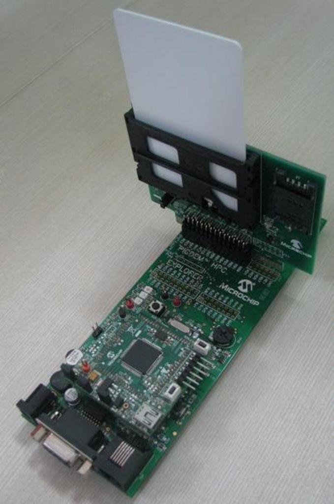
3) Insert the J4 port pins of SC (Smart/Sim
Card) PICTail Board in the J3
Configuration 2: Explorer 16
1)
Before attaching the PIM to the Explorer 16 board, insure that the processor
selector switch (S2) is in the “PIM” position as seen in the image below.
2)
Short the J7 jumper to the “PIC24” setting
3)
Be careful while inserting the PIC24FJ256GB110 PIM or any other appropriate PIM
into Exp 16 board. Insure that no pins are bent or damaged during the
process. Also insure that the PIM is not
shifted in any direction and that all of the headers are properly aligned.
4)
Short JP1 to SRC1 (i.e. RD1) or SRC2 (i.e. RB15) based upon the smart card
clock pin configured in the firmware: Example: - Short JP1 to SRC1 while using
PIC24FJ256GB110 demo and Short JP2 to SRC2 while using PIC32MX795F512L demo.
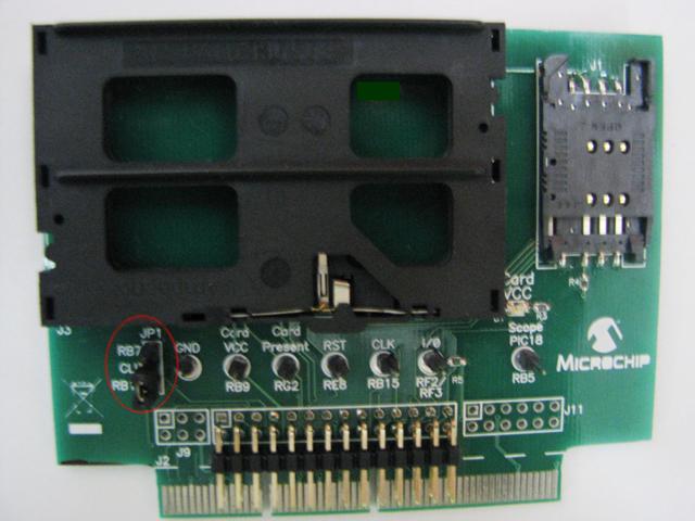
5) Insert the J2 slot of SC (Smart/Sim Card) PICTail
card into J5
Configuration 3: PIC18F14K50 + LPC Board
1)
Make sure that JP1 of SC PICTail card is left open. Make sure that J12 of LPC
board is left open. One side of J4 port pins of the SC (Smart/Sim Card) PICTail
Board matches with the J11
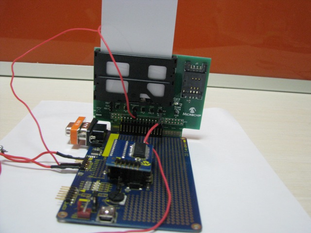
1) Short Tx & Rx line of the
UART (i.e. short pin 1 & pin 6 of J13 port using a wire in the LPC board) and
connect it to I/O pin of SC PICTail board.
2) Connect RB6 (i.e. pin 5 of J13
port in LPC board) to “Card Present” signal pin of SC PICTail board as shown
below.
Configuration 4: PICDEM FS USB
1) If using the PICDEM FS USB Demo Board, no hardware
related configuration or jumper setting changes should be necessary. The demo board need only be programmed with
appropriate firmware.
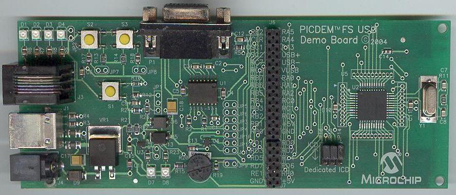
2) Don’t short the jumper at J11 port.
3) Insert the J2
To
run this project, you will need to load the corresponding firmware into the
devices.
The
source code for this demo is available in the “<Install Directory\Smart Card
Demo” directory. In this directory you
will find all of the user level source and header files, linker file as well as
project file for each of the hardware platforms. Find the project (*.mcp) file that
corresponds to the hardware platform you wish to test. Compile and program the
demo code into the hardware platform. For more help on how to compile and
program projects, please refer to the MPLAB® IDE help available through the
help menu of MPLAB (Help->Topics…->MPLAB IDE).
This demo uses the selected hardware platform as a Smart
card reader. The demo has to be run in the debug mode of MPLAB IDE. Please
refer “Configuring the Hardware” section for the bench setup connections.
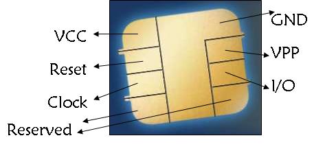
Smart Card consists of 8 pins namely:-
I/O: Input or Output for serial data to the integrated circuit inside the card.VPP: Programming voltage input (optional use by the card).GND: Ground (reference voltage).CLK: Clocking or timing signal.RST: Reset Signal to the Card.
VCC: Power supply input (optional use by the card).
Communication between the interfacing device and smart card
is done as per the following steps:-
·
Insertion
of the smart card in the slot.
·
Detection
of the smart card insertion by the microcontroller (interfacing device).
·
Microcontroller
does the cold reset of the smart card.
·
Answer
to Reset (ATR) response by the card.
·
PPS
exchange (if smart card supports it).
·
Execution
of the transaction(s) between the card & the interfacing device.
·
Removal
of the smart card from the slot.
·
Detection
of the smart card removal by the microcontroller.
·
Deactivation
of the contacts.
At the current times there are two communication protocols
that are in general use:-
·
T
= 0 asynchronous half duplex character transmission.
·
T
= 1 asynchronous half duplex block transmission.
The data transfers between the card and the terminal happens
on the single wire I/O line. The smart card library supports both T=0 & T=1
protocol.
Example code for T=0 cards:-
The demo executes the card commands namely SUBMIT CODE,
SELECT FILE, READ RECORD & WRITE RECORD. The command list can be extended further
as per the project requirement.
Example code for T=1 cards:-
The demo executes the "Get CPLC (Card Production Life
Cycle) data" command for T=1 java card. The command list can be extended
further as per the smart card manual and the project requirement.
The demo uses the signal connections between the smart card
& PIC micro port pins as per the below table:-
|
Signal Name |
PIC18F46J50 |
PIC18F87J50 |
PIC18F4550 |
PIC18F14K50 |
|
SIM_CARD_DET |
RB1 |
RB1 |
RB1 |
RB4 |
|
SMART_CLK |
RB2 |
RC2 |
RC2 |
RC2 |
|
SMART_I/O |
RC6,RC7 |
RC6,RC7 |
RC6,RC7 |
RB7,RB5 |
|
SMART_RST |
RB4 |
RB4 |
RB4 |
RC1 |
|
SMART_CARD_DET |
RB3 |
RB3 |
RB3 |
RB6 |
|
SMART_VCC |
RB0 |
RB0 |
RB0 |
RC0 |
|
Signal Name |
PIC24FJ256GB110 |
PIC32MX795F512L |
dsPIC33FJ128MC710 |
PIC24HJ256GP610 |
|
SIM_CARD_DET |
RB1 |
RB1 |
RB1 |
RB1 |
|
SMART_CLK |
RB15 |
RD1 |
RD1 |
RD1 |
|
SMART_I/O |
RC4, RF2 |
RF2 , RF8 |
RF2 , RF3 |
RF2 , RF3 |
|
SMART_RST |
RE8 |
RE8 |
RE8 |
RA12 |
|
SMART_CARD_DET |
RB0 |
RB0 |
RB0 |
RB0 |
|
SMART_VCC |
RB9 |
RB9 |
RB9 |
RB9 |
“SMART_CARD_DET”/”SIM_CARD_DET” signals indicate the
presence of Smart Card/Sim Card to the microcontroller. Either of one between
Smart Card & Sim Card has to be inserted in the Smart Card PICTail board.
If both the cards are inserted at a time in the PICTail card, then the demo
won’t work successfully.
If the user wants to connect the smart card signals to
different port pins of the micro, then he or she needs to modify the pin
mapping in “sc_config.h” file.
The demo
waits in the while(1) loop until the smart card is inserted in the smart card
connector slot. Once the card is inserted in the slot, ATR (Answer to Reset)
and PPS (Protocol & Parameter Selection) operations are performed. Then
after the execution of card commands is done as per the smart card manual
provided by the manufacturer. If the user inserts T=0 card in the slot, then
“SC_TransactT0” function is called & the result of the executed command
from the smart card is stored in “apduData”. If the user inserts T=1 card in
the slot, then “SC_TransactT1” function is called & the result of the
executed command from the smart card is stored in “apduData”. Variable
“cardResponse” stores the status codes & the length of the received data
from the smart card.
Note:
After initially being reset by the card reader, the smart card responds with a
string of characters known as the Answer to Reset, or ATR. These characters
consist of an initial character, TS, followed by a maximum of 32 additional
characters. Together, these characters provide information to the card reader
about how to communicate with the card for the remainder of the session. If the
card reader wants to modify any of these data transmission parameters in the
smart card, then it must perform PPS in accordance with ISO/IEC 7816-3 before
the transmission protocol is actually used.
For more
details about smart card communication using PIC microcontrollers, please refer
the application note AN1370
Troubleshooting Tips:
Issue
1: How to get the exact delays for Work Wait time functionality?
Solution: It is advisable to use Timers to generate the exact delays.
Trademarks:
The Microchip name and logo, the Microchip logo,
MPLAB, and PIC are registered trademarks of Microchip Technology Incorporated
in the
PICDEM and PICTail are trademarks of Microchip
Technology Incorporated in the
Microsoft, Windows, and Windows Vista are either
registered trademarks or trademarks of Microsoft Corporation in the
SD is a trademark of the SD Association in the
U.S.A and other countries
.JPG)
.JPG)
.JPG)
