Graphics PICtail™ Plus boards and PIC24FJ256DA210 Development Boards features flash memories. These are useful resources to store images, fonts and application data running on the mentioned demos. The following manual describes how these memories can be programmed.
All programming are initiated through a PC utility (memory_programmer.jar) provided with the Graphics Library Demos. You can find this utility in this path of your Microchip Application Libraries installation path:
..\<Installed Directory >\Microchip\Graphics\bin\memory_programmer
The hex files are generated by the “Graphics Resource Converter” located in:
..\ <Installed Directory> \Microchip\Graphics\bin\grc
Where: Installed Directory – is the directory where Microchip Application Libraries is installed (this includes the installation of the Graphics Library).
The demo projects that include flash programming are created to run on supported Microchip Demo Boards and development hardware. Pre-generated hex files are available on the "Precompiled Demos" sub-directory found in the demo directory. These hex files are generated using the alternative hardware profiles found in the sub-directory named "Alternative Configurations". Use the "Demo Compatibility Matrix" when running pre-generated hex files appropriate for your hardware.
This programmer allows downloading Intel Hex file into memory installed on selected hardware. Refer to the memory_programmer help file for details on the programmer utility operation. Instructions on how to install drivers for USB Device programming mode can also be found on this help file.
The figure below shows the possible combination of your hardware that requires programming. Depending on the hardware selected, the programming sequence will be the same but the required user interface (such as button press) may be different. Please refer to the different configurations below for details.
Configuration 1: PIC24FJ256DA210 Development Board
Configuration 1: Troubleshooting
Configuration 2: Troubleshooting
Configuration 1: PIC24FJ256DA210 Development Board
There are two flash memories on this board. The following steps sets up the Parallel or the SPI flash memory for programming and usage.
1) To use SPI Flash
a. Set jumper (JP23) to PMCS2-SPI
1) To use Parallel Flash
a. Set jumper (JP23) to PMCS2-PARALLEL
b. Depending on the memory range to be used
1. set jumper (JP11) to 1-2 when using 17 PMP address lines (PMP[16:0])
2. set jumper (JP11) to 2-3 when using 17 PMP address lines (PMP[17:0])
Note: Firmware must also initialize the EPMP SFRs to use the address lines. Please refer to EPMP FRM Chapter (DS39730a) for details.
2) To program (using Serial Communications)
a. Program the PIC24FJ256DA210 with the application hex code that contains the programming routine.
b. Connect the PIC24FJ256DA210 Development Board to the PC with a RS232 cable.
c. With the PIC24FJ256DA210 Development Board powered up, hold down button S2.
d. While holding button S2, push down and release button S4 (MCLR) to erase the data in flash memory then release the S2 button. This will put the application in programming mode.
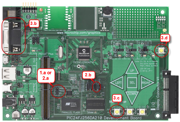
e. Run “memory_programmer.jar” on the PC side.
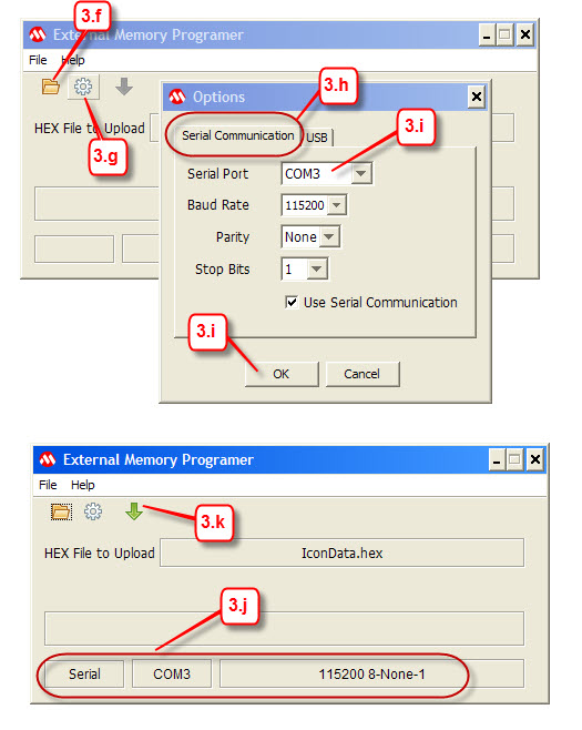
f. Browse the hex file that you want to program into the flash memory. Please refer to the specific demo manual for the actual hex file to program the flash memory.
g. Select the programming port to use.
h. Select the “Serial communications” tab.
i. Select the correct COM port connected to the PIC24FJ256DA210 Development Board and press OK.
j. Verify that the serial port is properly set to the correct COM port.
k. Press the Start icon. Programming should commence with the “Status” updating the number of packets sent.
Configuration 1: Troubleshooting
In some cases, programming will fail due varied reasons.
1. Only 1 line is transferred and the number of retries reaches the maximum. Check if the jumper (JP23) is setting the chip select to the correct flash memory.
2. When programming the parallel flash it always fails on a specific line number. Check jumper (JP11) if set to use 17 or 18 EPMP address lines.
3. “Programming Failed” message always appears. Check if the correct COM port is selected. This can be verified by looking at the Windows “Device Manager”. Verify the COM port under the “Ports (COM & LPT)”.
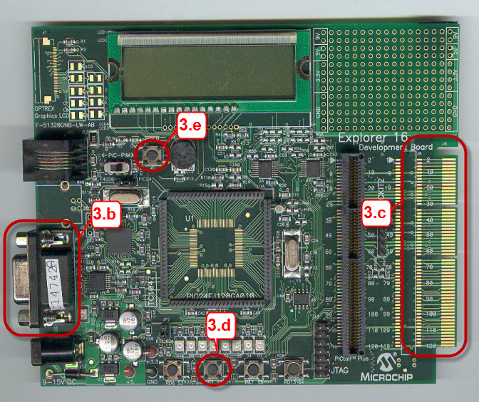
Configuration 2: Explorer 16
The explorer 16 can be connected to either the Graphics LCD Controller PICtail™ Plus SSD1926 Board or the Graphics PICtail™ Plus Daughter Board.
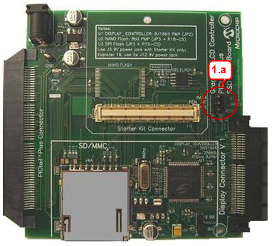
1) Graphics LCD Controller PICtail™ Plus SSD1926 Board use SPI Flash
a. Set jumper (JP3) to FLASH CS-RD1 to select SPI flash.
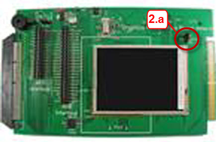
2) Graphics PICtail™ Plus Daughter Board use Parallel Flash
a. Set jumper (JP4) to FLASH CS-RD1 (the demos are configured to use this setting)
3) To program
a. Program the selected PIC device (PIM mounted on the Explorer 6 board) with the application hex code that contains the programming routine.
b. Connect the Explorer 16 Board PC with a RS232 cable.
c. Connect the Graphics LCD Controller PICtail™ Plus SSD1926 Board or Graphics PICtail™ Plus Daughter Board to the Explorer 16 Board using the J9 edge connector.
d. With the Explorer 16 Board powered up, hold down button S6.
e. While holding button S6 push down and release button S1 (MCLR) to erase the data in flash memory then release the S1 button. This will put the application in programming mode.
f. Run “External Memory Programmer.exe” on the PC side.
g. Browse the hex file that you want to program into the flash memory. Please refer to the specific demo manual for the actual hex file to program the flash memory.
h. Select the COM port connected to the PIC24FJ256DA210 Development Board.
i. Press the Start button. Programming should commence with the “Status” updating the number of transmitted lines. The utility is set to transfer at the baud rate of 115200.
Configuration 2: Troubleshooting
In some cases, programming will fail due varied reasons.
1. Only 1 line is transferred and the number of retries reaches the maximum. If using Graphics LCD Controller PICtail™ Plus SSD1926 Board, check if the jumper (JP3) is using the correct SPI flash memory chip select signal.
2. When using Graphics PICtail™ Plus Daughter Board, programming the parallel flash it always fails on a specific line number. Check the address lines of the parallel flash. One or more address lines may not be connected to the parallel flash properly.
3. “Programming Failed” message always appears. Check if the correct COM port is selected. This can be verified by looking at the Windows “Device Manager”. Verify the COM port under the “Ports (COM & LPT)”.